Designs Multi-cycle CPU by Logisim
Introduction
These projects were completed in my sophomore computer architecture course. As a new learner of computer architecture area, we simulated the logical circuit by Logisim. While in my free time, I designed a multi-cycle CPU by Logisim to meet my interests. This CPU use microprogrammed control, instead of hardwired control.
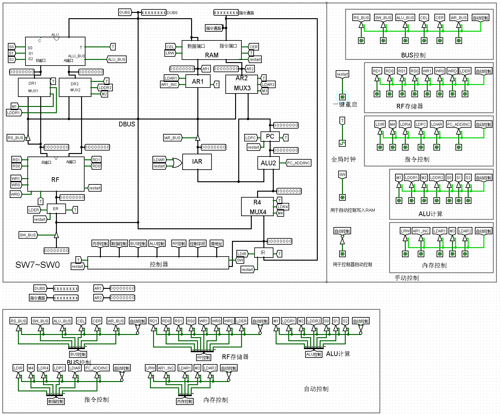
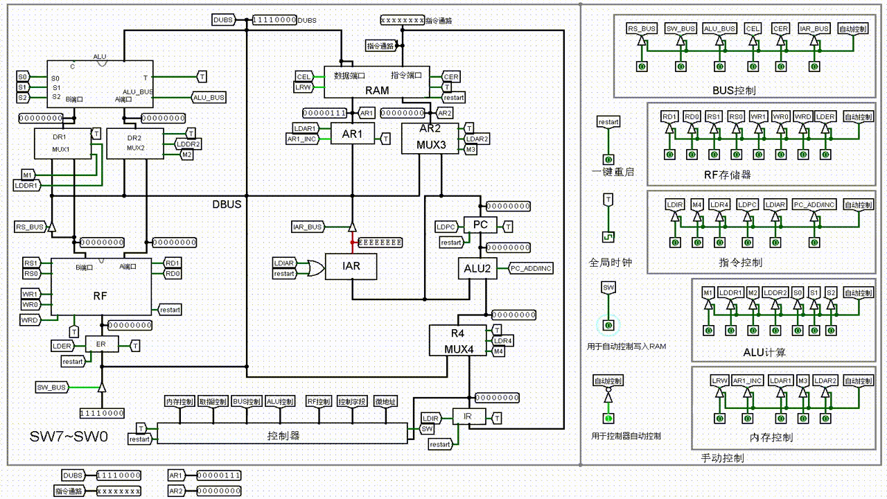
Here is the data bus of my CPU
While using it, you can save machine instruction in the RAM by using SW bus, and execute. There are total 5 types of basic instruction:
| Name | Code | Explain |
|---|---|---|
| Load | 1001 xx __ | Load the next 8-bit number from RAM into register. The last 2 bits is the register name |
| Add | 1000 __ __ | Add numbers from two register, write back to the register named in the last 2 bits |
| Minus | 1010 __ __ | Minus numbers from two register, write back to the register named in the last 2 bits |
| Show | 1011 xx __ | Show the number in the register into data bus |
| Halt | 1111 xx xx | Stop the micro program controller |
After wrote some instruction into RAM, and click the “Disable writing into RAM” button, you can operate the clock and see the change of data bus. Program Counter (PC) register will auto-increment, and load instruction one by one into microprogram branching system to analyse the next microprogram address. Then the microprogram will control the tri-state gate switch to drive the program execution.
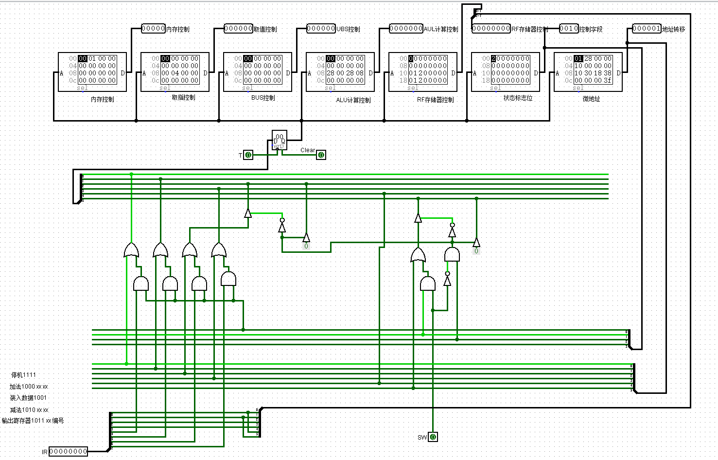
Here is the microprogram branching system.
A Brief Example
1. Load instruction into RAM
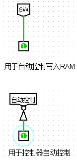
Turn on this two button. The first button used to allow next data write into RAM, and the second button used to turn on the micro program controller. If you don’t turn on the second button, you will need to control each switch on the data bus by yourself.
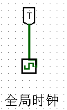
Click the clock button 4 times, to boot the system.
Adjust SW bus input, make it become 1001 xx 00 (1001 stand for load instruction, xx stand for the number in this bit will not change the result, and the last 2 bits 00 stand for register 00), and click the clock button 4 times. Because logisim is not a real circuit simulation, there will be some transfer delay, so I have to do some trick to solve this problem. Therefore, you will need to click 4 times to load the first instruction code into RAM.
Then, adjust SW bus into 0000 1110 (just a number), and click the clock button twice.
After that, you will adjust SW bus input, and make it become the following status, and click the clock button twice each time:
- 1001 xx 11 (Load the next number into register 11)
- 0111 00 00 (Number 0111 0000)
- 1000 11 00 (Add register 11 and register 00, write the result back into register 00)
- 1011 xx 00 (Show the number of register 00 into the data bus)
- 1111 xx xx (Halt)
Because there are total 7 instructions, therefore, you will get number 7 in the RAM address selecting register
2. Execute the Code
Turn off the button that used to allow next data write into RAM, and start the clock, you will get the next result
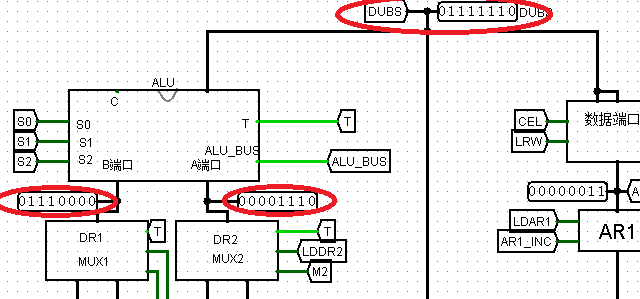
0111 0000 and 0000 1110 will be added successfully, and the result 0111 1110 will appear in the data bus.
Here is the final execution process
To see more about the project, please click here.